CHAPTER 2
LOGIC CIRCUITRY, RAM, AND THE CPU.
CMOS LOGIC CIRCUITS:
While it is not necessary to be an electronics technician, it is a good idea for a programmer to have at least some idea of the hardware that underlies assembly language and other code, as this helps to fill a gap in the understanding that might contribute to a lack of confidence in gaining an understanding of the physical reality that underlies the creation of program code.
As mentioned before, the hardware is designed to represent the two characters that make up the binary number system by means of the presence of a voltage, which represents the binary character 1, or
the absence of a voltage, which represents the binary character 0. In the transistor circuitry described below, the transistors are used essentially as switches which switch voltages on or off, and thus transmit the equivalent of binary characters from inputs to outputs.
The name CMOS refers to the nature of the transistors used in these circuits. Its full title is actually CMOSFET, which stands for 'complementary magnesium oxide silicon field effect transistors'. The two transistors, A
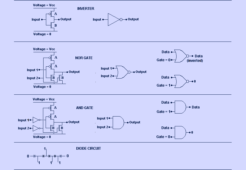
and B, in the inverter circuit shown, are of opposite types and work together in a complementary manner, which is why you have the designation CMOS, rather than MOS, with the C standing for 'complementary'.
The inverter circuit, which is the simplest, works as follows: if the input is at zero volts, the transistor A is turned on, and is like a short circuit, connecting the output terminal to the top voltage line, while transistor B is turned off, disconnecting the output terminal from the bottom voltage line. Thus, the output terminal is at the same voltage as the top line, Vcc. If, however, the input is at the voltage Vcc, the transistor A is turned off, disconnecting the output terminal from the top voltage line, while transistor B is turned on, connecting the output terminal to the bottom voltage line. The output terminal voltage is thus at the same voltage as the bottom voltage line, 0 volts.
Since the circuit works on the basis of two possible voltage conditions of a terminal, Vcc or 0 volts, these two conditions can be referred to as 1 or 0 respectively, in this way representing the condition of a terminal by means of a binary numerical designation. This is how electronic circuitry is designed to be associated with the binary number system.
The above description of the inverter circuit shows that the circuit 'inverts' the 'binary' value of the input. That is, if the input value is 0, the output value is 1, and if the input value is 1, the output value is 0
The inverter illustration is necessary to understand the working of the two cmos logic gates illustrated below it: the NOR gate and the AND gate.
The NOR gate is a simple development of the inverter circuit. There are two A transistors in series, which means that if either of them is switched off, the output is disconnected from the top voltage line, Vcc. If this is the case, it means that one of the two B transistors will be switched on and will short circuit the output terminal to the bottom voltage line, at 0 volts, even if the other B transistor is switched off. Thus, the output terminal will be at 0 volts. This will be the case if either of the input terminals, 1 or 2, is at voltage Vcc. The only case in which the output terminal will be at voltage Vcc is the case where both inputs, 1 and 2 are at zero volts. In binary terminology, the only case in which the output has a value of 1 is when both inputs have a value of 0. In any situation, where either or both inputs have the value 1, the output has the value 0. That is, the output is at 1 only when neither input 1 NOR input 2 is at 1; hence the name NOR gate.
Further on I give an illustration as an example of how cmos circuits can be used, in a computer, to create a readout of data in a RAM (random access memory) memory location in response to an address selected by the computer CPU (central processing unit).
The AND gate circuit is the same as the NOR gate circuit, except that the inputs, 1 and 2, have inverter circuits connected to them, so that the inputs, 1 and 2, of the AND gate are the inputs to the two inverters. Since inverters invert the values of the inputs, two 1 values on the inputs to the AND gate will cause two 0 values on the inputs to the nor circuitry, causing the output terminal to the AND gate to be 1. In accordance with the working of the nor circuitry described above, the only case in which the output of the AND gate is at 1 is the case in which both input 1 AND input 2 have the value 1, hence the name AND gate.
The use of the concept of a 'gate' can be seen from the illustrations to the right of the NOR and AND gate circuits. The diagrams shown immediately next to the INVERTER, NOR gate and AND gate circuits are used to represent these circuits in cmos logic diagrams. From the working of the NOR gate circuitry, as described above, the output terminal can have a value 1 only if both inputs have a value 0. Thus, if input 2, for example, is at the value 1, input 1 can be changed from 0 to 1 and back, without any change to the output value. However, if input 2 is held at the value 0, the output will change with any change to input 1, and will display the inverted value of input 1. Here we can see that terminal 2 is being used as a kind of switch that allows or prevents data getting through from terminal 1 to the output. That is, the circuit is being used as a kind of 'gate' that can be opened or closed to either allow or prevent data passing through to the output. Hence the concept of a logic 'gate'. The illustrations on the far right show the terminals being used in this way.
It remains only to mention the diode circuit shown at the bottom of the diagram. The diode symbol has the shape of an arrow pointing in the 'forward' direction. It can be understood simply as a device that allows a voltage (more accurately, a current) to be transmitted through it in the forward direction but blocks a voltage in the reverse direction. That is, if the voltage Vcc is applied to the diode input, a voltage Vcc will appear on the output, but if the voltage of the input is 0 and the voltage Vcc is applied to the output, the voltage on the input will remain at 0. Thus, in the diode diagram above, the voltage, or binary value 1 will be transmitted in the forward direction through the shaded diodes but will be blocked by the reversed, unshaded diodes.
A CMOS LOGIC MEMORY CIRCUIT:
We now have all we need in order to be able to understand the following illustration of the use of logic gates in an actual logic circuit as would be used in a computer.
The circuit diagram, below, is a simplified example
of the kind of circuitry that would enable a computer CPU to read a value stored at a RAM memory location, selected by a binary number referred to as an 'address'.
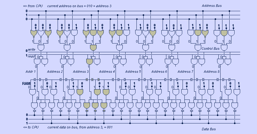
Communication between the CPU and RAM is via 3 buses: an address bus, a data bus, and a control bus. In the diagram, the address and data buses have three lines each, and the size of RAM memory is only 17 bits, or individual binary values, with only 8 possible addresses. Since, however, this circuit is complicated enough with only this much memory, the reader can imagine the complexity involved in trying to illustrate an actual RAM circuit with 32 lines or more on the address bus and 32 lines also on the data bus, with the size of memory being possibly of the order of 800 megabits. The number of gates involved would require a diagram of such a size that it would have to be spread out on the floor like a large map to see only a part of it. The above diagram, however, is sufficient to illustrate how the circuitry works, since an actual circuit is merely an extrapolation based on essentially the same design principles.
When a program code tells the CPU to fetch the value stored at a particular address in RAM, the CPU puts the address on the address bus. In the diagram, the CPU has put the binary address 010 on the address bus. The actual addresses from which a particular address is to be selected are hard wired into the row of gates immediately below the address bus. That is, the binary address values are permanently fixed at the values shown. There are 8 such addresses: 000, 001, 010, 011, 100, 101, 110, 111. These are simply a binary number count from 0 to 7. They act as gate values which allow or prevent the data on the address bus getting through to the AND gates below them. The AND gates have three inputs each, and the output of any of these gates will have a value 1 only if all three inputs have the value 1. This will occur only if the corresponding three address gates all have output values of 1, and this, in turn, will occur only if the data on the address bus is the same as the fixed address values on the gate inputs. Thus, in the illustration, address number 010, the second address, is the only one that will have a value of 1 on the output of its 3-input AND gate. This value is transmitted to three AND gates immediately above the data bus, and switches them on. The same output value is also transmitted via the diodes to the three RAM AND gates that have the data stored on their inputs. These three AND gates are thus also switched on. This allows the data stored in memory to be transmitted through the two lower sets of AND gates, thus allowing it to appear on the data bus. All the AND gates that correspond to the other addresses are not switched on, so that their stored data does not affect the values on the data bus.
The lowest set of AND gates, immediately above the data bus, is necessary to enable some of the memory storage gates to be connected to either the first line of the data bus, or the last line. This is because the addresses are separated by only two bits, whereas the data read out consists of three bits. That is, the last bit at one memory address is the first bit of the next, i.e., the data overlaps from one address to another. This corresponds to the real case in which the distance fixed between possible addresses is 8 bits, or one byte, whereas the data read out onto the 32 bit data bus from any one address will be 32 bits, thus over-lapping 4 possible addresses. Therefore, some individual bits of stored data will have to be able to be connected to 4 different lines on the data bus, depending on their location relative to the addressed byte.
Connecting an address to the address bus alone does not specify whether the data at the specified address is to be read onto the data bus, or written from the data bus into the address. The purpose of the control bus is to determine which of these alternatives applies. One of each of the pairs of AND gates immediately below the control bus are switched on by a 1 appearing on either the read or write line of the control bus. In the illustration, the read gates are all switched on, and the write gates are switched off. The write gates would be connected to alternative circuitry, not shown, which would be the reverse of the read circuitry shown, and would cause the data on the data bus to be transferred into, rather than out of, the memory location specified by the address on the address bus.
Finally, it is worth mentioning how the above working of RAM circuitry is connected with assembly language instructions involving memory and memory addressing.
A programmer assigns a name to a memory location that the program code will need to use. Thus, the memory location in the above diagram, identified by the binary address 010, might have been named by the programmer as 'LengthA', for example. The programmer, of course, knows nothing about the address 010, because this is assigned to the name LengthA, by the system, only when the program, or exe file, is actually run by a user, and may be different each time. The programmer therefore has to assign only the name LengthA and the size of data to be associated with it, such as byte, word, or dword, leaving the system to take care of the actual address each time. If the programmer uses the following assembly language instruction in his code:
mov eax, [LengthA]
LengthA will be translated by the system to the binary number 010, and the resulting, effective instruction, mov eax, [010], will cause the CPU to put the address 010 on the address bus, thus reading the data at that address onto the data bus. The CPU will then put the data on the data bus into the register eax (the value 001 in the illustration). If, however, the programmer writes the following instruction:
mov eax, LengthA
without the brackets, the CPU will put the address value 010 itself directly into eax, and will not read the contents of the address via the data bus. Here, of course, I am ignoring that eax is a 32 bit register, and that the above instructions are 32 bit instructions, and not 3 bit instructions, but, apart from this, the description is sufficient to give the reader an understanding of how these processes work.
The CPU itself, of course, has a similar kind of logic circuitry wired to correspond to all the different kinds of assembly language instructions available. It is not my purpose to attempt to describe that circuitry but, based on the foregoing illustration of RAM circuitry, the reader will, I hope, be able to form a qualitative concept of the physical hardware that lies behind assembly language code and, indeed, but more indirectly, that of other, higher level languages.
Part I: Part I Introduction
Chapter 1: Binary numbers, code, and procedures
Chapter 3: Assembly Language
Chapter 4: Assembly Language Code example
Chapter 5: Macros and HLA
Chapter 6: HLA code example
Chapter 7: The Windows operating system
Chapter 8: Data Structures
Chapter 9: How to Create a Windows Program
Chapter 10: How to Create an Exe File
Chapter 11: Structured Programming and OOP
Part II: Part II Introduction
Chapter 12: Debugging a Windows Program Code
Chapter 13: Painting the Window Client Area
Chapter 14: Creating Window Menus
Chapter 15: How to Create Toolbars
Chapter 16: How to Create Popup Menus
Chapter 17: About the Windows Clipboard
Chapter 18: How to Create Bitmaps
Chapter 19: Icons and the Ico Format
Chapter 20: Common Dialog Boxes
Chapter 21: Working with Files
Chapter 22: Scrollbars and Scrolling
Chapter 23: How to Send Data to the Printer
Chapter 24: Miscellaneous Topics
© Alen, August 2013
alen@alenspage.net
Material on this page may be reproduced
for personal use only.